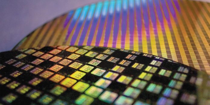
When it comes to the bleeding edge of semiconductor technology, TSMC’s still got their A-game going. According to an Anandtech report, TSMC has been making great progress on the development of the 3nm EUV process node. They’ve already engaged early customers to help with “technology definition.”

TSMC has refused to out details about their take on the 3nm node, nor about specific improvements over the 5nm node. However, they’re confident that their approach to 3nm will deliver a “very good solution” to early-bird clients. They’ve also confirmed that their 3nm node will be based on completely new process technology–it won’t be a simple iteration over their 5nm approach.
Samsung is also set to get in on the 3nm game but they’ll be using a different process called Gate-All-Around MBCFET, what they’re calling 3GAEE (which is certainly easier to write than that earlier word soup).

The bigger question, though, is just when can we expect these parts in volume? Moore’s law has been dead for some time and we’ve already taken far longer to reach 7nm than early predictions claimed. And, perhaps even more importantly, what comes next? When we’re manufacturing in the sub-3nm range, there are literally not enough atoms to make functioning transistors. Do we move to quantum computing? Or use photonic signaling in place of electricity?
Further Reading:


