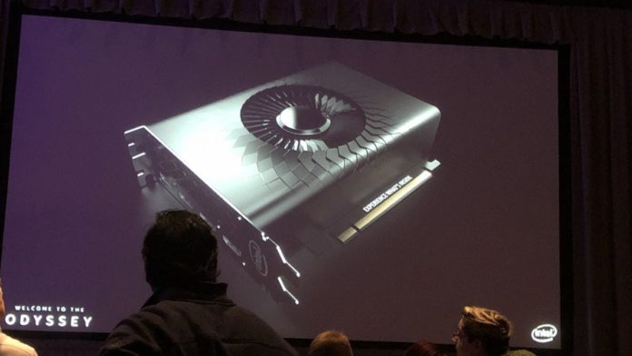
It seems like the Intel Xe GPU development or project Odyssey has been almost been finalized. As per a leak, an internal event dubbed “Xe Unleashed” was recently held with all the key players including Bob Swan, Raja Koduri and even reps from Asus and other AIBs present. The slides from the presentation have been leaked and guess what the ‘e’ in the Xe stands for? The GPU count. Yes, we’re talking about multi-GPU products here. The flagship will be a dual-GPU offering an insane 66.8 Teraflops (of HP?) compute performance, thanks to a brand new architecture and 4D memory.

Looking at the leaked specifications, we can see that the GPUs will be based on the 7nm node, which Intel has yet to come up with. The flagship Intel Xe 2 GPU will boast a total of 12288 stream processors, with each internal chip packing 6144. These shaders or cores will have a base clock of 1600 MHz with a boost of 2718 MHz. And here’s the biggie, the GPU will leverage Intel’s 4D XPoint memory and that too 32 GBs of it. The total bandwidth seems to be pegged at 8TB/s, and all of this meaty hardware culminates into a total processing performance of 66.8 TFLOPs although I think this is the half-precision peak. The TDP is rated at 350W with a Direct3D 14_2, API capability.
Confirmed: NVIDIA’s Tom Petersen is Indeed Joining the Intel GPU Team
ASRock’s GPU Business Suffers due to Crash in CryptoCurrencies
Intel Xe 2 Dual GPU with 32 GB VRAM and 8TB/s Bandwidth to Cost $699
Here’s the best part, as per the source, the GPU will be priced quite aggressively with a launch price of $699. This puts the Intel Xe 2 GPU in the same price slab as the GeForce RTX 2080 and the Radeon VII, only with a lot more processing power and memory.

I’m fairly certain something is off here. Either the purported price is a fluke or the 66.8 TFLOPS of performance refers to the half-precision compute peak. This would make sense considering that the AI and neural network industry is more suited for it. And given the excessive memory and bandwidth, it’s almost certain that the Intel Xe 2 will target this lucrative market. Gamers will probably get the second priority, but that remains to be seen.
Multiple Xe GPUs Unified by the One API for Enhanced Scaling
Traditionally multiple GPU solutions like SLI and XFX get very limited support from both developers and OEMs alike due to the small user-base. Scalability and efficiency have always suffered as a result, but Intel claims to have the solution to that. The Intel Visual technologies Team has come up with the One API that will lie between the DX3D layer and the GPU(s). This makes multiple GPUs appear as a single unit to applications and as such developers don’t have to optimize their applications for multi-GPU configs.
AMD Radeon RX Navi, Ryzen 3000, EPYC Rome CPUs to Be Announced at Computex 2019

To maximize yields, Intel is going with four 400mm dies instead of one 800mm. However, the first generation Xe 2 will pack two 600mm dies, thereby reducing wastage but retaining the raw processing power. Looking at Intel’s roadmap, it’s rather ambitious with the flagship Xe products going from two GPUs for the Xe 2 in 2020 (July 31st) to eight GPUs for Xe 8 by 2023. This is all a bit too much to take in, but the slides appear to be quite legit.
Intel is venturing into unknown territory with the MCM approach. It has never been done before so either it’ll fall flat or Intel will reign supreme in the GPU space in the coming years.
WccfTech claims that the card will have two operating modes. A base mode wherein the GPU(s) will run at relatively lower speeds and a turbo boost mode, which when coupled with a liquid cooling solution should allow core clocks of up to 2.7 GHz. Again, all this is a bit hard to digest, but considering this will be Intel’s very first encroachment into the discrete GPU space it makes sense to go all-out and let’s not forget that team blue is much bigger than both NVIDIA and AMD combined.
PS: The source claims that the first reference model will be fabbed in partnership with Asus.
Read more:


It’s an April Fools joke.
Need that 4 dimensional memory to bend time.
nice try?
Isn’t this a April Fool’s Joke?…
😉
Given the date of release of such news, it’s hard to believe
Dear Intel, ” yawn ” .