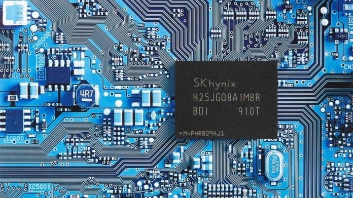
SK Hynix unveiled its HBM2E DRAM today with industry-leading bandwidth by 50% and twice as much capacity as compared to last gen. The new HBM2E standard supports over 460GB/s bandwidth based on 3.6 GB/s performance per pin with 1,024 data I/Os
SK Hynix achieves this feat by making use of TSV (Through Silicon Via) technology to vertically stack a maximum of 8 16Gb chips, resulting in a dense bundle of 16GB of data. HBM2E is interconnected closely with GPUs and logic chips, separated by only a few micro-meters, resulting in faster and more efficient data transfer. It is built from the ground-up to support supercomputers, high-end GPUs, machine learning and AI systems which require the highest level of memory performance.

For the sake of comparison, the RTX 2080 with 8GB GDDR6 of memory delivers 448GB/s of bandwidth while the new HBM2E memory offers twice as much capacity with a significant increase in performance at the same time. The current GPU which offers the highest memory bandwidth is the AMD Radeon VII at 1,024 GB/s. Using SK Hynix’s new memory, it can offer up to 1,840GB/s of bandwidth, making it faster by almost 80%.
The first SK Hynix HBM2E chips will begin mass production in 2020, at the start of the 4th Industrial Era.
Further Reading:


