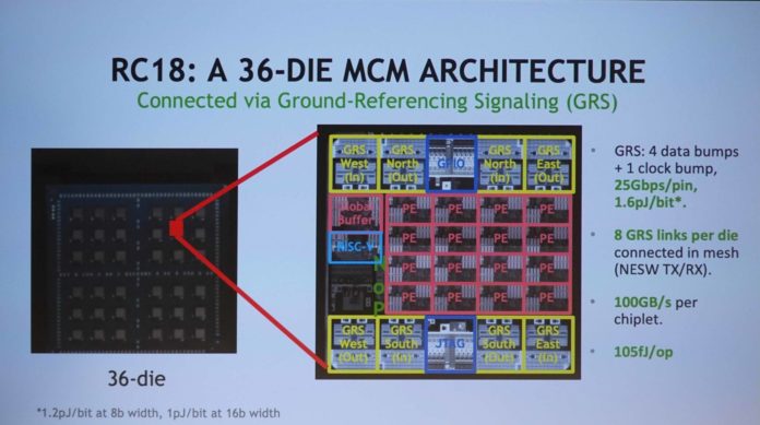
Moore’s law may well and truly be dead as we see more and more semiconductor companies ditching the traditional monolithic chip design in favor of a modular approach. This is becoming vital for chipmakers in order to improve the power efficiency of their designs. Intel has been stuck on 14nm since forever and while TSMC has fared much better, there’s no denying that shrinking transistors is getting harder by the day. Using such new design methods, chipmakers are hoping to reduce the intra-chip power draw to 1 picoJoule/bit or less. As such, the bi-directional peak power for 1TB/s transfer will be

At the 2019 VLSI Symposium, earlier this month, NVIDIA shared technical details about its new intra-chip transmission technology called Ground-Referenced Signaling (GRS) which it has implemented on its 2018 Research Chip or “RC18”. This should allow low power data transfer among the 4 dies viz. North, South, West, and East, on the same RC18 package. NVIDIA estimates that a 16-bit wide interface on their 16nm RC18 will land them at their targeted 1pJ/bit energy consumption. For comparison, AMD’s 14nm Infinity Fabric with a 32-bit wide interface consumes twice the energy at 2pJ/bit. If these claims by Nvidia turn out to be accurate then AMD could have a hard time competing as their recently launched 7nm Navi GPUs already consume a bit more power than similarly performing 12nm Turing cards.
A modular approach should also lead to a more scalable design making it easier to expand upon.


This is a very brief overview of Nvidia’s MCM approach. If you are curious to know more, please refer to this article.
Read more:


